三星将在2022 VLSI上发表18篇论文
VLSI研讨会将于6月12日至17日在檀香山的希尔顿夏威夷村举行。三星将在会议上发表18篇论文。
其中在DRAM存储器类别中,三星将发表 "A 16 GB 1024 GB/s HBM3 DRAM with On-Die Error Control"。
三星的第三代10纳米DRAM(1z)具有更高的系统可靠性、可用性和可维修性(RAS)的性能,主要针对汽车、工业和数据中心应用。
为此,他们采用了一种新的片上纠错(ECC)方案,可以同时纠正16位字错误和2个单独位错误,并将其纳入新版 "高带宽内存-3"(HBM3)DRAM中。
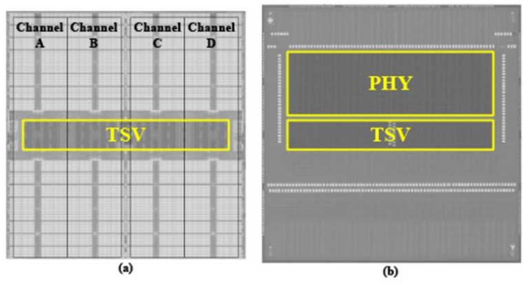
三星的HBM3芯片的显微照片:(a)核心和(b)缓冲buffer
在每个单独的DRAM芯片上进行本地修正,而不是访问堆栈中的其他部分,从而减少了延迟,并将引脚数据速率从上一代的5Gb/s/引脚提高到8.0Gb/s/引脚,使每个内存的总内存带宽达到1024GB/s。并在一个16GB的DRAM模块中得到了证明。
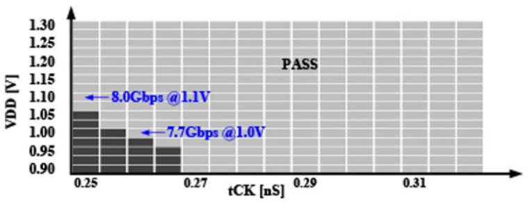
三星的HBM3芯片的实测时钟频率
三星的3纳米栅极环绕FET(GAA FET)技术在 "A 3nm GAAFET Analog Assisted Digital LDO with High Current Density for Dynamic Voltage Scaling Mobile Applications "中得到了展示。
这里讨论了模拟辅助数字LDO,它提供了高电流密度的电力输送,该设计具有主动的电源噪声消除和CPU内核的快速瞬态负载检测。
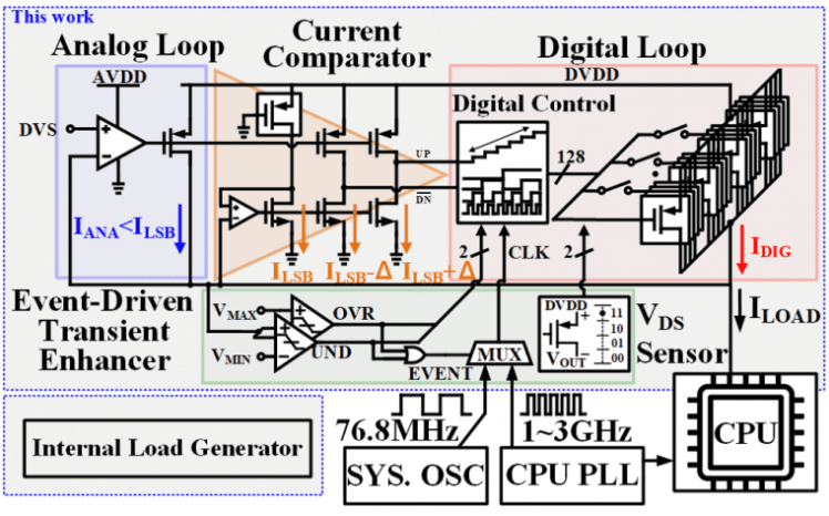
三星提出的用于移动SoC应用的混合LDO结构
这种混合LDO设计在<1 mA到1.4 A的负载范围内实现了精确的调节,在1 ns内对1 A的动态负载只有38mV的电源下降。
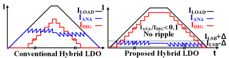
传统和混合的GAAFET LDO的负载曲线
此外,还有一篇关于 "A 0.6μm Small Pixel for High Resolution CMOS Image Sensor with Full Well Capacity of 10,000e- by Dual Vertical Transfer Gate Technology"的论文。
三星公司利用双垂直转移门(D-VTG)技术,开发了一种使用0.6μm像素的200Mp图像传感器原型,其全电荷井容量(FWC)为10,000e。与单垂直转移门相比,D-VTG的FWC增加了60%,并且由于转移门电压的可控性提高,转移性能也得到了改善。
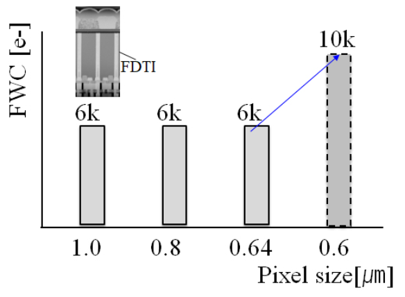
三星根据像素大小的全电荷井容量
通过调整VTG的间隙、深度和锥度斜率来优化光电子传输,如下图所示。
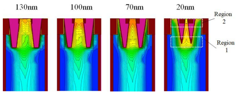
转移门的电位曲线与间距的关系
此外,其他收录论文还包括了:
C10-1? A 12-bit 8GS/s RF Sampling DAC with Code-Dependent Nonlinearity Compensation and Intersegmental Current-Mismatch Calibration in 5-nm FinFET
C10-3? A 0.56mW 63.6dB SNDR 250MS/s SAR ADC in 8-nm FinFET
C11-5? Fully Integrated 2×2 MIMO Real Simultaneous Dual Band WiFi CMOS Power Amplifiers With a Single Inductor Multiple Output Supply Modulation Technique
C14-2? High Efficiency 29-/38-GHz Hybrid Transceiver Front-Ends Utilizing Si CMOS and GaAs HEMT for 5G NR Millimeter-Wave Mobile Applications
C15-2? A 32 Mb Embedded Flash Memory based on 28 nm with the best Cell Efficiency and Robust Design achievement featuring 13.48 Mb/mm2 at 0.85 V
C17-1? A 40-Gb/s/pin Low-Voltage POD Single-Ended PAM-4 Transceiver with Timing Calibrated Resetless Slicer and Bidirectional T-Coil for GDDR7 Application
C16-3? An Automotive ASIL-D Safety Mechanism in ADC and DAC for Communication Application
C18-5? Palm-sized LiDAR module with III/V-on-Si optical phased array
C19-3? A 12-bit 10GS/s 16-Channel Time-Interleaved ADC with a Digital Processing Timing-Skew Background Calibration in 5nm FinFET
C22-4? A 0.7 mm2 Power Management Unit for Implantable Electroceutical Device with a
91.4 % Peak Efficiency Buck-based Hybrid Step-up and -down MISIMO Converter
C24-4? 4-nm Voltage Auto-Tracking SRAM Pulse Generator with Fully RC Optimized Row Auto-Tracking Write Assist Circuits
TFS1-2? Prospective Innovation of DRAM, Flash, and Logic Technologies for Digital Transformation (DX) Era
T8-5? ? Advanced novel optical stack technologies for high SNR in CMOS Image Sensor
T10-1? Standard Cell Design Optimization with Advanced MOL Technology in 3-nm GAA Process
T10-4? Comprehensive Feasibility Study of Single FIN Transistors for Scaling Both Switching Energy and Device Footprint