通富微电框架类封装
Production Overview ? ? ? ? TFME is able to provide Solder bump, Cu pillar bump and Gold bump for customer to meet different requirement. ? ? ? ? ? ? ? ???Solder bump? ? ? ? ? ? ? ? ? ? ? ? ? ? ? ? ? ? ? ? ? ? ? ? ? ? ? ? ??Cu pillar bump??? ? ? ? ? ? ? ? ? ? ? ? ? ? ? ? ? ? ? ? ? ? ? ? ? ? ? ??Gold bump ? ? ? ? ? ? ? ? - Wafer size: 8 inch / 12 inch?? ??? ? ? ? ? ? ? ? ? ? ? ? ? ? ? ?- Wafer size: 8 inch / 12 inch? ? ? ? ? ? ? ? ? ? ? ? ? ? ? ? ? ? ? ? - Wafer size: 8 inch / 12 inch ? ? ? ? ? ? ? ? - Bump qty: 2892(MAX)? ? ? ? ? ? ? ? ? ? ? ? ? ? ? ? ? ? ? ?- Bump qty:? 1500 pin (max)? ? ? ? ? ? ? ? ? ? ? ? ? ? ? ? ? ? ? ? ?- Bump qty: 4091/pin (max) ? ? ? ? ? ? ? ? - Structure: 0P1M~2P2M? ? ? ? ? ? ? ? ? ? ? ? ? ? ? ? ? ? ? ?? - Structure: 0P1M~1P2M? ? ? ? ? ? ? ? ? ? ? ? ? ? ? ? ? ? ? ? ? ? ? -?Structure: 0P1M~1P1MBump Series

? ? ? ? ? ? ? ? - Body size:? 0.7*0.76~10.7*10.7 mm? ? ? ? ? ? ? ? ? ? ? ?- Body size:? 1.0*1.5~10*10mm? ? ? ? ? ? ? ? ? ? ? ? ? ? ? ? ??? - Structure: 0P1M~1P1M?
? ? ? ? ? ? ? ? - RDL L/S: min.5um/5um? ? ? ? ? ? ? ? ? ? ? ? ? ? ? ? ? ? ?? ? ?- RDL? L/S: min. 5um/5um? ? ? ? ? ? ? ? ? ? ? ? ? ? ? ? ? ? ? ?? ?? - Bump L/S: min.10um/8um?
Solder bump & Cu pillar
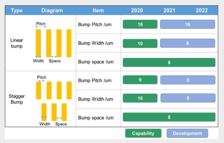
Process Capability & Design Rule
Gold bump
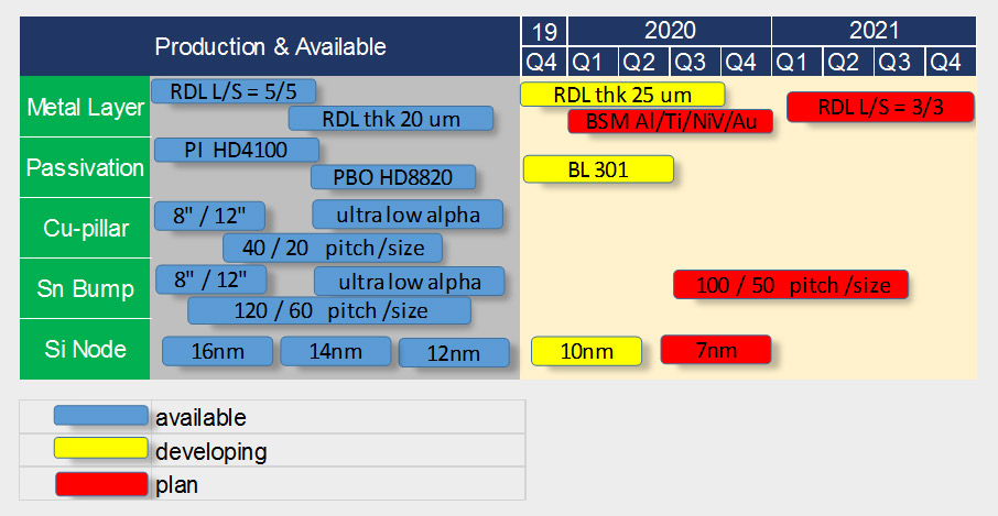
Reliability Test Standards
Solder bump & Cu Pillar bump
Gold bump

Shipment Packing

WLCSP Series
Production Overview
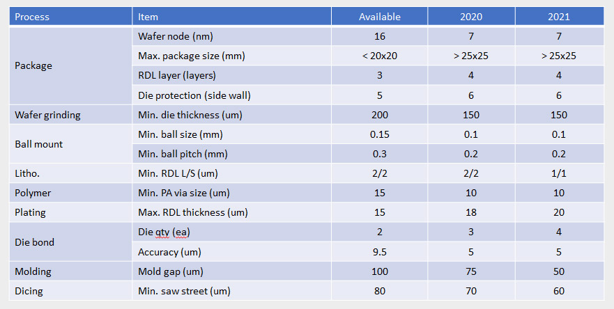
? ? ? ? TFME offers? various Wafer Level CSP product to customer including Fan in type and Fan out type.
Feature
? ? ? ? ? Fan in WLCSP? ? ? ? ? ? ? ? ? ? ? ? ? ? ? ? ? ? ? ? ? ? ? ? ? ? ? ? ? ? ? ? ? ? ? ? ? ? ? ? ? ? ? ? ? ? ? ? ? ? ? ? ? ? ? ? ? ? ? ? ? ? ? ? ? ? ? ? ?Fan out WLCSP
? ? ? ? ?- Ball count : 2~309? ? ? ? ? ? ? ? ? ? ? ? ? ? ? ? ? ? ? ? ? ? ? ? ? ? ? ? ? ? ? ? ? ? ? ? ? ? ? ? ? ? ? ? ? ? ? ? ? ? ? ? ? ? ? ? ? ? ? ? ? ? ? - Ball count : 36 ~203?
? ? ? ? ?- Structure: 1P1M~2P2M? ? ? ? ? ? ? ? ? ? ? ? ? ? ? ? ? ? ? ? ? ? ? ? ? ? ? ? ? ? ? ? ? ? ? ? ? ? ? ? ? ? ? ? ? ? ? ? ? ? ? ? ? ? ? ? ? ? ?- Structure: 1P1M~3P3M
? ? ? ? ?- Body size:? 0.6*0.3~7.6*7.6mm? ?? ? ? ? ? ? ? ? ? ? ? ? ? ? ? ? ? ? ? ? ? ? ? ? ? ? ? ? ? ? ? ? ? ? ? ? ? ? ? ? ? ? ? ? ? ? ? ? ? ? ? ?- Body size: max 20*20mm
? ? ? ? ?- RDL L/S: min.5um/5um?? ? ? ? ? ? ? ? ? ? ? ? ? ? ? ? ? ? ? ? ? ? ? ? ? ? ? ? ? ? ? ? ? ? ? ? ? ? ? ? ? ? ? ? ? ? ? ? ? ? ? ? ? ? ? ? ? ? ?- RDL L/S: min.2um/2um
Process Capability & Design Rule
Fan in WLCSP
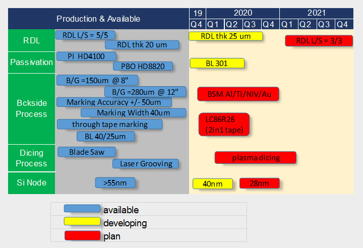
Process Capability & Design Rule
Fan out WLCSP
Reliability Test Standards

Shipment Packing

COGCOF Series
Production Overview
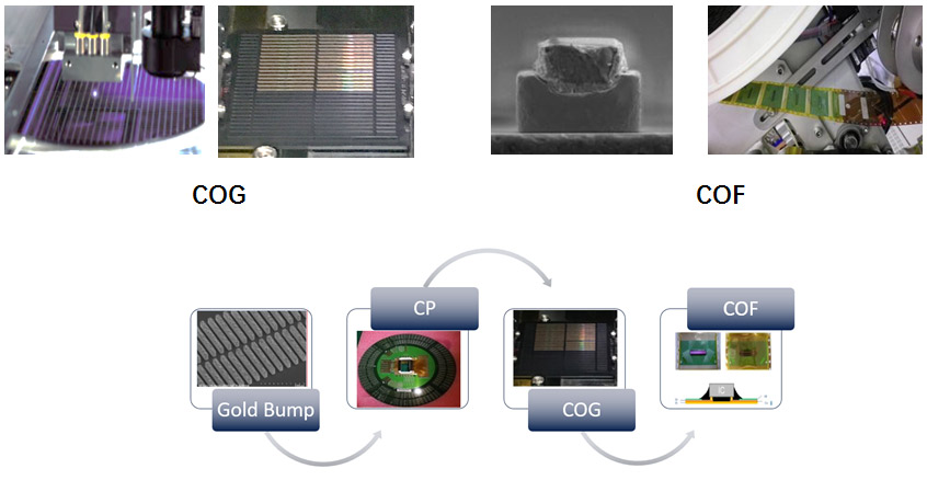
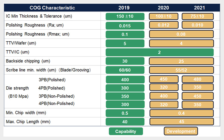
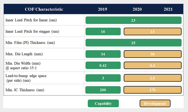
? ? TFME is able to provide COG (Chip On Glass) and COF (Chip On Film) services for gold bump drive IC?based on customer requirement.??
? ??
Process Capability & Design Rule
COG
Process Capability & Design Rule
? ? COF
Reliability Test Standards
?
Shipment Packing

FCBGAFCLGA Series

Production Overview?
Flip Chip interconnection, also knownas Controlled Collapse Chip Connection, C4, has been identified as a high performance packaging solution to meet the growing need for products with increased electrical performance, high I/O, and high system reliability as a replacement for conventional wire bond process. Utilizing whole die area as for electrical connection, substrate I/O per unit exponentially increased vs. perimeter wire interconnection technology.?
Flip chip interconnect also allows direct connection with on-die power planes which enables increased electrical performance including increased switching speed and more efficient power distribution to the IC performance at lower operating voltages.?
TF-AMD Flip Chip are assembled with single unit laminate which is the highest routing density through build-up technology to maximize the device performance &conventional ceramic substrate for reliability enhanced package solution. Combined with Flip Chip interconnection, TF-AMD provides optimal design flexibility for final package design& product format to fit an end user requirement.?TF-AMD offers Flip Chip BGA packages with ball counts up to 3000 & PGA package up to 2000
Application?
Flip Chippackage is considered one of the most established industry platform applicable for high pincount and/or high performance ASICs. Large body FC BGA/PGAs provide package solution forComputing (microprocessors / graphic, server), gaming,high bandwidth networking/Communicationdevices. Combined with Flip Chip technology &BGA/PGAlead format, TF-AMD help to enable SMT and also pin insertion application.
Features?
Flip Chip BGA/PGA Packaging?
Package Types: Bare die, Stiffener, Lidded (Top hat & flat top)?

Wafer Node 314/16nm ELK(extreme low K) qualified, 7nm in development.?
Package sizes from 12mm to 55mm (75mm in development)?
Die area up to 800mm^2?
Lead Free, Eutectic, High-Pb bump for Flip Chip connection?
Passive component size down to 01005?
High thermal performance solution using Indium metal TIM?
Substrate?
? ? ? ? ? ? ? ?o? ? 4 – 18 layers laminate build up?
? ? ? ? ? ? ? ?o? ? Coreless, 0.2mm, 0.4mm, 0.8mm, 1.0mm available?
? ? ? ? ? ? ? ?o? ? High CTE ceramic / LTCC alumina ceramic?
? ? ? ? ? ? ? ?o? ? BGA / PGA?
Footprints Pitch?
? ? ? ? ? ? ? ? o? ? BGA : 0.5mm, 0.65mm, 0.8mm and 1.0mm?
? ? ? ? ? ? ? ? o? ? PGA : 1.0mm, 1.27mm?
Other Option?
? ? ? ? ? ? ? ? o? ? Multi-die capability?
? ? ? ? ? ? ? ? o? ? Die binning to waffle pack up to 256 BINs?
Flip Chip BGA/PGA Test?
Test Product Engineering?
? ? ? ? ? ? ? ? o? ? TF-AMD test provides a competitive test solution to our customers ranging from test development, platform conversion, and product maintenance and test data analysis.?
? ? ? ? ? ? ? ? o? ? The team has rich test development experience of various product portfolio, including high-end digital, mix-signal, SOC and high speed products.?
Adding Value to Customer?
? ? ? ? ? ? ? ? o? ? Reduce customer overhead by outsourcing projects / tasks to avoid maintaining a large scale of dedicated team?
? ? ? ? ? ? ? ? o? ? Incorporate industrial standard through leveraging best known method from our database & continuous cost saving by driving test time reduction, yield improvement?
Service Solutions?
? ? ? ? ? ? ? ? ?o? ? Wafer Sort test development?
? ? ? ? ? ? ? ? ?o? ? Final Test development?
? ? ? ? ? ? ? ? ?o? ? Low cost platform conversion?
? ? ? ? ? ? ? ? ?o? ? Multi-site enablement?
? ? ? ? ? ? ? ? ?o? ? Burn-in capabilities?
Test Development Experience?
? ? ? ? ? ? ? ? ?o? ? CPU, APU, GPU?
? ? ? ? ? ? ? ? ?o? ? Chipset?
? ? ? ? ? ? ? ? ?o? ? Digital Audio?
? ? ? ? ? ? ? ? ?o? ? Baseband?
? ? ? ? ? ? ? ? ?o? ? Microcontroller?
? ? ? ? ? ? ? ? ?o? ? LCD Driver?
? ? ? ? ? ? ? ? ?o? ? Touch Panel Driver?
ATE platforms and products?
Reliability Test Standards?
Design Rule?
Top Hat Single Piece Lid?

Lid size=substrate size-0.2mm?
Standard foot sizes?
? ? ? ? ? ? ? ? ? ? ? ? o? ? 2mm for 15-25mm body?
? ? ? ? ? ? ? ? ? ? ? ? o? ? 3mm for 27-31mm body?
? ? ? ? ? ? ? ? ? ? ? ? o? ? 4mm for 33-50mm body?
Max 3mm on all four sides (UF will flow under the bend/slant of the HS). Extended design rule allow Max. 2.5mm for the body size ≤31mm?
Lid is centered?
Cavity depth for 12inch wafer SPL is 0.8mm and total thickness is 1.3mm?
? ? ? ? ? ? ? ? ? ?? ? ?o? ? TIM Thickness target: 40um (Max. 100um)?
? ? ? ? ? ? ? ? ? ? ?? ?o? ? Adhesive Thickness target: 120um (Max. 200um)?
? ? ? ? ? ? ? ? ? ? ? ? o? ? Lid manufacturing tolerance: +/-50um?
Body size<31mm support bare die structure (without stiffener/lid construction)?
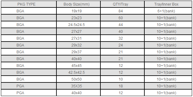
Packing & Shipping (in house standard)?
BGA / PGA (Tray)?
当前位置:首页?>?产品技术?封装品种?>FCCSPFCLGA Series Production Overview ? ? ? ? TFME offers various FCCSP and FCLGA package based on customer different requirement. Features Process?Capability & Design Rule Reliability Test Standards Shipment PackingFCCSPFCLGA Series

- SiP (FC + SMT + Wire bond) available.
- CUF, MUF available.
- 7N/12N/14N/16N wafer node mass production
- Various substrate technology qualified including SAP, MSAP, ETS, MIS and SLP.
- Fully Turnkey for wafer bumping, probing, assembly, FT available.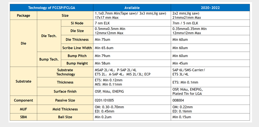


WBBGAWBLGA Series
Production Overview
? ? ? ? TFME offers various WBBGA and WBLGA package based on customer different requirement.

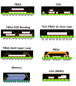
Features
- 1.1x0.7 mm to 21x21 mm Package
- 0.2mm to 1.0mm C Mold Chase
- 01005 Components SMT
- 0.3x0.3 mm Small Die?
- 1-6 Layer Substrate
Process Capability & Design Rule
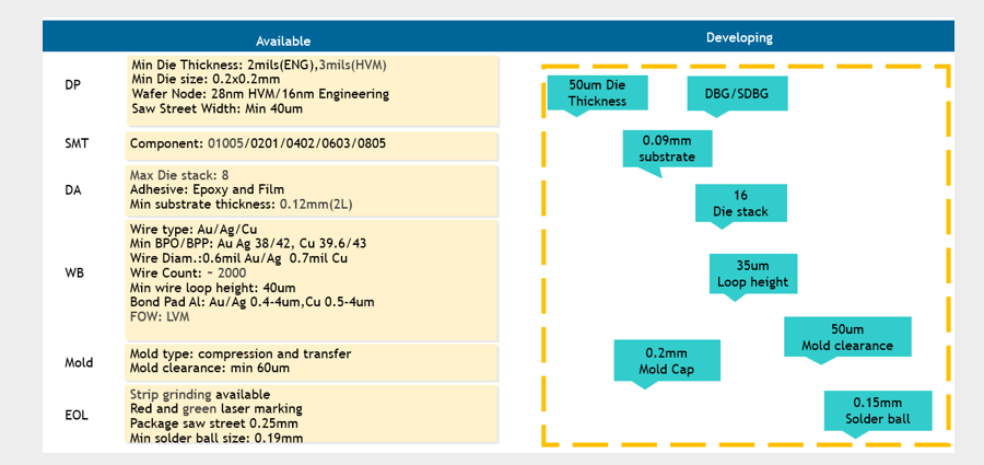
Reliability Test Standards

Shipment Packing

